Dream protoboard? (not breadboard, the kind you solder to) #1654
Replies: 83 comments
-
|
Posted at 2015-03-27 by @gfwilliams Sounds like a great idea. When we come up with a good design I'd happily get a bunch made at DirtyPCBs and sell them. My personal preference would be for connected blocks of 3 pins. Maybe spaces for not just an SOIC8 but an SOIC16 too (on the other side?) and maybe slightly longer tracks to allow the SMD FETs to be soldered on too (that FET+SMD resistor thing is awesome). Also if you're going for Pico support then a space for a JST connector (so it can be used with the Pico soldered down) and pads for a MAX1555 LiPo charger might make sense? And mounting holes would be cool too. |
Beta Was this translation helpful? Give feedback.
-
|
Posted at 2015-03-27 by alexanderbrevig I'd like edge headers in 2mm and 2.54mm pitch with a trace to a neighbour through hole pad (I.e exactly what the Espruino has on the edge opposite to the usb) so it's easy to route i/o to a header/plug. Having a plethora of various SMD fooprints would be awesome too! For me the optimal would be to have through hole pads next to the smd pads (will constrain space though, and again this is so I could use jumper wires for quick prototyping). Maybe it would be an idea to make two variants, one for SMD and one for through hole. It would also be cool to allow the protoboards to connect to eachother with say an edge connector and using the pcb as a plug into the next. I have a lot of surplus SOT-23 and 0603 components, so thouse would be a high priority for me but probably not for the next guy. Something like: This board has a lot of options, and a nice way of doing multiple pin counts: |

Beta Was this translation helpful? Give feedback.
-
|
Posted at 2015-03-27 by @gfwilliams Another option is to have a 0.1" board (maybe with SOIC pads) and then have a second optional board full of snap-out adaptors that convert the more strange footprints back into 0.1"? |
Beta Was this translation helpful? Give feedback.
-
|
Posted at 2015-03-27 by DrAzzy My thinking so far is for most of the surface to be stripes of two rows of 3 or 4-hole, each on either side of of SOIC pads (probably SOIC-16's, since 2 of those are an SOIC-8). Note the extra pad at the end of the rows of 4 - that's an SMD pad... though maybe I should omit that, and just rely on the normal spacing, and let the SMD cover part of the last hole. I'll need to do a few mockups this weekend with printout. There's also the question of whether to expose the copper between each hole in a row, and even whether to put that copper between the holes in a row on both sides, or only on one side - I think a trace could be squeezed between them - maybe for routing SPI or I2C? But maybe that wouldn't be a good place to route data lines. It would probably make sense to have some areas at least where there's 3 wires (SPI or I2C + spare) with multiple taps on it, near the IC area. My plan is for there to be a hole for most, if not all pins - I don't want to make many assumptions about what specific part is going in any place, except for the most common-of-common (like a pile of SOT-23 with the sources all on ground or something). I was thinking I need some spots with SOT-23-6 pads, maybe some of those weird SM-8 packages, thjat look like SOIC, only a bit smaller (I have a few parts in that). Re: that red board - when was the last time you wanted to solder down something with pins on 4 sides, and it was something that would be sensible to slap onto protoboard? Sure, there are a million and one lovely sensors and stuff, but not in packages that you can really hand-solder onto protoboard. I agree on some 2mm pitch near the edge for interfacing. |
Beta Was this translation helpful? Give feedback.
-
|
Posted at 2015-04-04 by DrAzzy 2x ssop-28 (back), 2x soic-24W/N + 2x msop16 (not a real package - I think msop stops at 10) with long pads for weird small stuff, three through hole per. I think I'm going to have combo 5050 (like the leds) SOT-23-6 footprint, probably on the top (leds should point up, right?), with narrow SOIC on the back. I'm going to have pads for esp8266 smd version, so the antenna hangs of the side (there will be rows of holes under it), like the end of the Pico has to) |
Beta Was this translation helpful? Give feedback.
-
|
Posted at 2015-04-05 by alexanderbrevig Just stumbled upon this https://www.kickstarter.com/projects/658903329/perf-the-perfboard-reinvented some good ideas there I think :) Though I'd post just in case you get some inspiration. |
Beta Was this translation helpful? Give feedback.
-
|
Posted at 2015-04-06 by DrAzzy
Somehow I need to cram in fets, interfacing, and some regulators in the remaining space. |

Beta Was this translation helpful? Give feedback.
-
|
Posted at 2015-04-06 by alexanderbrevig Nice work man! I'll buy some off you if you plan on selling. Or order some if you release Gerbers. Looking good! Would you consider breaking those 4-long rows around the Espruino into 2x2 with no solder mask between the two groups? Then it would be easy to lead f.ex a resistor over to some other device. And it would also be easy to make a solder bridge if one needs all three pins on an Espruino pin. |
Beta Was this translation helpful? Give feedback.
-
|
Posted at 2015-04-07 by DrAzzy Good call. Done. I will either sell them or release the gerbers, or maybe do DirtyPCB's $1 referral thingie. Or maybe @gfwilliams might be better placed to sell the Espruino ones. I think if these are good, I'll do a non-Espruino one (ie, for AVR/etc) with ISP headers for common AVR chips, and maybe TQFP pads for 328/1284. Would probably be easier to move. Unless anyone sees any problems or room for improvement here, I'm going to send this off to dirtypcb's today or tomorrow, and I'm gonna do the non-shitty shipping I think, to get it in a reasonable length of time so I can assess whether to get a resellable quantity quickly. |

Beta Was this translation helpful? Give feedback.
-
|
Posted at 2015-04-07 by alexanderbrevig Your power buses are floating? I guess you may be thinking that you wire them to where you want? (so there's no mask over? that's probably what the //// are all about....) I would like to see a header exposing the lines from the pads of the power jack as well. For testing it would be nice to simply make a banana->jack and use a bench power supply. Currently it seems hard to do a direct tap? One more thing, if one wanted to do a large-ish LED project (and thus high current on the power jack) then thicker traces for it may be a good idea. Lastly (if I were to sell something) I'd replace all straight angles with 45* like you do for most traces. If only to never hear anyone complain or ask why it's designed as it is. I'm sure it would have no practical implications but it might if someone wanted to make say an Espruino controller GPS Disciplined Oscillator. Disclaimer: I am a beginner, think of these comments as questions. Seems very good. I'd buy some. |
Beta Was this translation helpful? Give feedback.
-
|
Posted at 2015-04-08 by DrAzzy Ya, the busses are exposed. The power jack pins go out to sue of those rows of three near the jack. I'll do a check for asymmetrical routing, but I'm not going to do Kickstarter, so I'm not too concerned. :) Good catch on the trace width for power jack. |
Beta Was this translation helpful? Give feedback.
-
|
Posted at 2015-04-08 by the1laz This is looking great, I'd be interested in grabbing some too. It'd be great for all the projects I'd like to try with surface mount parts, I've usually stuck with through hole up until now. |
Beta Was this translation helpful? Give feedback.
-
|
Posted at 2015-04-08 by DrAzzy |

Beta Was this translation helpful? Give feedback.
-
|
Posted at 2015-04-08 by @gfwilliams Looks great! Just some ideas:
Looks like I'll probably start some kind of online shop for the adaptor shims, so I'd be very happy to sell this with some kind of referral? About the 45 degree angles - I still think it's a non-issue for normal GPIO lines (I imagine it helps stuff like clock lines). But yes, it won't stop people complaining whenever they see one :) I still want a PCB design tool that'll do routing with nice curved lines that automatically bend around vias and things. |
Beta Was this translation helpful? Give feedback.
-
|
Posted at 2015-04-08 by alexanderbrevig Looking very good! @gfwilliams "I still want a PCB design tool that'll do routing with nice curved lines that automatically bend around vias and things." Altium does this. You can either drag and it will place tracks according to rules where it can find path. You can also enable push tracks which will push tracks. Then push vias which will also push vias, lastly a god mode push which will replace everything to let your track through. It's powerful for tight routing! https://youtu.be/VhPk3J1WcpE?t=4m11s see it in action here (this guy uses 45* but you can change rules to use rounded (also min/pref/max radius). :) |
Beta Was this translation helpful? Give feedback.
-
|
Posted at 2015-06-01 by DrAzzy I've put it up for sale on Tindie... https://www.tindie.com/stores/DrAzzy/ Still awaiting admin approval on the listings, ofc. Presently, I don't have a good way of doing international shipping - There's gotta be a way to ship a single bare board like it was a letter - it's under the weight and thickness limits and all, and until I can do that, I can't ship internationally for a sane price. |
Beta Was this translation helpful? Give feedback.
-
|
Posted at 2015-06-01 by @gfwilliams I don't know how it works in the US, but in the UK we have various sizes and price bands - sizes are here If you can fit within them then there's no problem - just stick the right postage on it and you're sorted? OSHPark sends internationally in all-plastic padded bags (probably the same thing they send across the US in). I've never had any problems with the stuff when it's arrived. |
Beta Was this translation helpful? Give feedback.
-
|
Posted at 2015-06-02 by DrAzzy They've been Admin-Approved (except for one, which mysteriously hasn't gotten the approval yet. They dribble out the approvals too) I've still not yet worked out international shipping, but I've got domestic shipping sorted, I think. I also realized I need some decent envelopes. |
Beta Was this translation helpful? Give feedback.
-
|
Posted at 2015-06-19 by DrAzzy International shipping is sorted out now. I've got some more cool stuff going up on there friday assuming the approval gods work with haste - MOSFET breakout boards loaded with logic level FETs, capacitive proximity sensors. |
Beta Was this translation helpful? Give feedback.
-
|
Posted at 2015-06-19 by @gfwilliams Ohh, those sound good. For the Pico, or general purpose? |
Beta Was this translation helpful? Give feedback.
-
|
Posted at 2015-06-19 by DrAzzy They're general purpose - but obviously, MOSFETs that work with 2.5v Vgs are a lot more useful for 3.3v microcontrollers than 5v ones. I've got SOT-23 MOSFET breakouts (about the size of a TO-22o package), and a larger 4-channel one with 20A mosfets on it. The touch/proximity sensor is an MTCH101 based device, real simple, and you can use whatever you want as the sensor, as long as it's metal. Wires, screen, foil, coke cans... It's open drain output, and has a pullup resistor on board. |
Beta Was this translation helpful? Give feedback.
-
|
Posted at 2015-07-10 by DrAzzy |


Beta Was this translation helpful? Give feedback.
-
|
Posted at 2015-07-10 by @gfwilliams Nice! Wow, there's a lot of stuff on that one board! Slightly surprising seeing that big flash(?) chip on the back of the EasyVR board too! |
Beta Was this translation helpful? Give feedback.
-
|
Posted at 2015-07-10 by alexanderbrevig Really nice :) Here is the datasheet on the parallell flash chip. HAve you tried it @drazzy ? |
Beta Was this translation helpful? Give feedback.
-
|
Posted at 2015-07-10 by DrAzzy I've tested parts of it, but still don't have major pieces of the software together, and some of the wiring still needs to be done. The indicator LEDs (WS2812's - I need indicators, but I can't spare the pins for normal LEDs) and I2C devices still need to be wired in. It's getting a BMP180 (maybe here I'll be able to make data come out of it?), color sensor (the good one, with I2C output, in DFN-6 package - why the chinese module people only make breakouts for the crappy ones with frequency output is a mystery to me). Chip on the bottom is an 24-series EEPROM (I thought I'd never get to use up those TSSOP EEPROMs!) Yeah - it's a shame there isn't more memory on the EasyVR. I'd kill for more commands - it's capped at 32 total, I think due to memory limitations, which goes really fast. Currently for testing, it's all powered off the USB (3.3v devices running off the Pico's regulator). When it's done, though, I'll remove the jumper, and connect the 3.3v regulator from the power section to the Vcc rail, and the 5v regulator on the bottom to the Espruino's BAT_IN (so that will be supplying the Pico, and the 5v RF comms board (this should be fine talking over serial, since the Pico's pins are 5v tolerant) It also gets a keypad (connection point is under the wizio550), and that'll be mounted on a little piece of aluminum that will hide the top half of the device. Somewhere I need to fit a PIR motion sensor too. The intended functionality is:
|
Beta Was this translation helpful? Give feedback.
-
|
Posted at 2015-07-12 by DrAzzy
|


Beta Was this translation helpful? Give feedback.
-
|
Posted at 2015-07-13 by DrAzzy All the parts are on and basic hardware functionality checks out. RF comms seems to be busted, but I suspect that's a problem with the software on the RF controller - need to take a look. That or I got the tx/rx backwards or something dumb like that. The TCS34725 works, and I submitted a pull request for the (very simple) module for it. |
Beta Was this translation helpful? Give feedback.
-
|
Posted at 2015-07-14 by @gfwilliams Great! Yes, I'll try and get that pulled in today :) |
Beta Was this translation helpful? Give feedback.
-
|
Posted at 2015-07-14 by DrAzzy Thanks. Got the RF comms working mostly - that was a bug in AzzyRF which I've got sorted now. |
Beta Was this translation helpful? Give feedback.
-
|
Posted at 2017-02-03 by OwenBrotherwood
A link to such for SOIC/SMS footprints in relation to nRF5X? |
Beta Was this translation helpful? Give feedback.
-
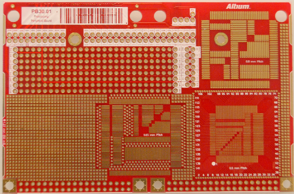
Posted at 2015-03-26 by DrAzzy
So, we all build prototype-grade circuits...
Which means you end up building "on" something.
Most people who've used breadboard for a while quickly come to hate it for it's poor reliability (also odd things - apparently the capacitance is so high that some breadboard arduino's won't work unless you omit the loading caps on the crystal). Of course, any SMD stuff needs to be on breakout board. So breadboard, not so great.
Strip-board is better, but the kind with long strips requires you to cut copper with xacto-knives, and the result looks like utter shit. You're dependent on breakout boards for any SMD stuff, except that you can sometimes lay SMD resistors/caps between strips.
An even better kind is what I call "proto board" - this is like strip-board, but the strips are already broken up into groups of 4, so it's like breadboard. It may have traces running between rows of pins carrying power or ground.
I have some very nice protoboard from back when state of the art equipment was DIP parts, and that's how it was prototyped. What makes this nicer, is that it's double-sided, with plated through holes - this makes it better than most of the available protoboard. Ofc, same problem with SMD's.
There is also a garbage form of protoboard which has NO connections between the pins, so all it does is stick things down, so wiring is a nightmare. This stuff belongs in the trash. Unfortunately, is is VERY common.
Now, as it happens, Gordon has seen the light (as we all know very well; Espruino is awesome). Beyond that, also in prototyping, on the original board, with his integrated SMD prototyping area. Which is just wonderful, except for the little detail of it being attached to a $40 Espruino. My prototypes aren't that good ;-)
But imagine for a moment a hybrid prototyping board. This would have rows of pins in groups of 4 in some sections for general work and DIP stuff, but also some SOIC16 pads, with the pins broken out to strips with holes. Some SOIC8 ones too. Pads for some common transistors. Power and ground (maybe even an extra power rail) distributed around the board. The board could be designed so that "sections" with specific functions could be chopped off if not needed.
What has brought this to my mind again now is that DirtyPCBs will make 10 boards 10cm on a side (ie, just under 4x4) for $25. That's affordable, and a 4x4 hybrid protoboard would (designed well) make several devices.
What sorts of outlines and general considerations does this bring to people's minds?
Ideas on how to arrange things for maximum versatility for someone who works with both SMD and throughhole parts?
Obviously, it's going to have a pico header (using the pins, so you can use the space under it if the project doesn't call for a pico.
The motivation for this was the fact that it's pretty common for me to want, say, an SMD chip wired up to a few SOT-23's and some passives, with a regulator, and right now that's meant breakout boards and protoboard and ratsnests of wires, or me giving up and doing a home-fab board.
In the SMD areas, you could have different stuff on the two sides, too...... I like this.
Beta Was this translation helpful? Give feedback.
All reactions